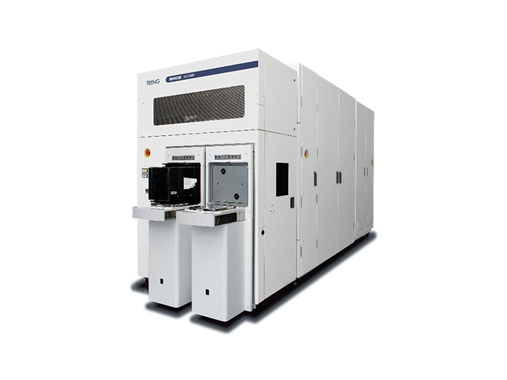

Key Features
- High-resolution electron-beam technology with a minimum detectable defect size down to 1 nm.
- Fast, large-area scanning to improve inspection throughput.
- Supports inline inspection requirements.
- AI-based defect classification to enhance review efficiency and consistency.
- Supports automated operation and SECS/GEM communication for factory integration.
Applications
- Wafer defect inspection and analysis
- Wafer process anomaly monitoring
- Photomask and pattern transfer quality control
- Yield analysis for advanced processes (e.g., EUV, 3D IC, etc.)
About TORAY (Toray Engineering)
Toray Engineering Co., Ltd. was established in 1960, initially providing plant construction and production equipment maintenance for Toray Industries, Inc. As a member of the Toray Group, Toray Engineering has 11 subsidiaries in Japan and overseas, and is currently engaged in three major business areas: Engineering, Electronics, and Environment & Energy.